These devices are technical means used in the synthesis of insulating coatings, new polymers, dielectrics and semiconductors. For work in the field of microelectronics are often used:
- diffractometers;
- atomic absorption spectrometer;
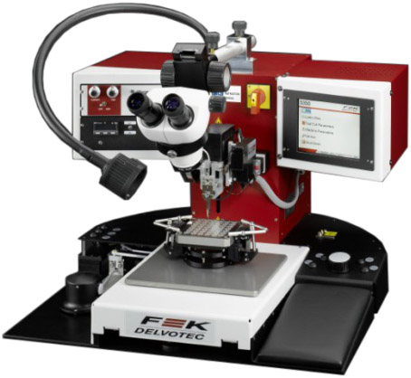
- microwelding installations;
- centrifuges, etc.
These installations will make it possible to fully equip the laboratory at a manufacturing enterprise, at a research institute.
Micro welding machines 53XX BDA

- welding method: Ball welding, wedge-wedge, ball-wedge
- Wire type: 17.5…75 µm, gold, aluminium, tape 30×12.5…250×25 µm, spool 2″ or 1/2″
- Z-axis drive: 60 mm, pitch 1 µm
- Y axis drive: 4 mm, pitch 2 µm
- Work table and manipulator: Frame size 18×18 mm, mechanical drive with X/Y displacement factor 1:7
- Programmable clamping force: 5… 150 sN
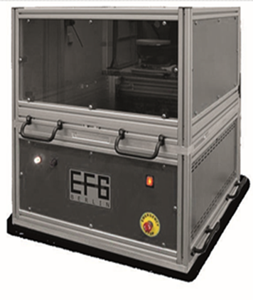
X-ray diffractometers for determining orientation in single crystals

The DDCOM X-ray diffractometer for determining the orientation in single crystals using the Omega-scanning tool allows one revolution in a short time, up to 5 seconds and with a high accuracy of up to 1/100 ° to determine the orientation of the crystal lattice in 3D, which is 200 times faster than the common Tehta-scan method. scan (Theta scan)
Specifications
- X-ray source 30W air-cooled X-ray tube, Cu anode
- Detectors Two scintillation detectors
- Sample holder Turntable, 0.01° accuracy, sample positioning and marking tool
- dimensions 600mm×600mm×850mm
- Weight 80 kg
- Source of power 100-230V, 100W, single phase
- Room temperature ≤ 30 ° C
- Required space: about 1.5m x 1.5m, computer space required
Peculiarities
- Automatic, high-precision determination of the full orientation of the lattice of a single crystal in 3D.
- High productivity (more than 250 samples per shift) and reliability allows it to be used in industry for mass production 24 hours a day, 7 days a week.
- The modularity of the design makes it possible to design and manufacture automated complexes for determining the orientation for specific customer tasks, the development of automatic sample preparation devices, special equipment and sample holders.
- Convenient and easy to operate.
- Low operating costs.
- Azimuth settings and crystal orientation marking
- High accuracy up to 1/100°
- Latest and user-friendly software
- Suitable for a wide range of sample sizes and weights: platinum 1” ÷ 12”, crystals up to 20 kg, (single crystals up to 400 mm long can be measured.)
- Allows you to measure materials:
- Ag, Au, Ni, Pt
- Cube / random unknown orientation: Si, Ge, GaAs, GaP, AlAs, AlP, InP, NaCl, AgCl, CaF 2
- Cube / special orientation: Ag, Au, Ni, Pt, GaSb, InAs, InSb, AlSb, ZnTe, CdTe, Si 3 C, PbS, PbTe, SnTe, MgO, LiF, MgAl 2 O 4 , SrTiO 3 , LaTiO 3
- Hexagonal / Trigonal: silicon carbide SiC 2H, 4H, 6H, 15R, GaN, ZnO, LiNbO 3 , SiO 2 (quartz), Al 2 O 3 (sapphire), GAPO 4 , La 3 Ga 5 SiO 14
- Rhombic: Mg 2 SiO 4 , NdGaO 3
- Other materials according to customers’ requirements
- Suitable for research and product quality control.
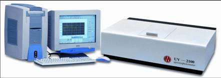
UV/Vis Spectrophotometer UV-2100

Chemical analysis in various fields of industry, education and science.
Specifications of UV-2100 spectrophotometer
- Spectral range, 190-910 nm
- Wavelength setting accuracy over the entire range, ±0.3 nm
- Width of the selected spectral interval, 0.1, 0.2, 0.5, 1.0, 2.0 nm
- Range of measured transmittance, optical density, -0.300 - 4.000 A
- Photometric accuracy ±0.3%T (0-100%T), ±0.002A(0-0.5A), ±0.004A(0.5A-1A)
- Photometric reproducibility 0.001A(0-0.5A)
- Working mode T, A (-0.3-4A), E
- Baseline linearity ±0.001A
- Scattering, at a wavelength of 340 nm, <=0.05%
- External output RS 232
- Light source: UV - deuterium lamp, Visible range - tungsten halogen lamp
- Zero signal drift, 0.0004 Ah
- Photometric linearity at 1.0A, ±0.001A
- PMT detector
- Power supply, 220/50 Hz, 110/60 Hz
- Power consumption, no more, 400 W
- Weight, 45 kg
